
CES is here and we were almost losing our collective minds over "will they or won't they" commentary regarding peeps from the next generation of consoles. Of course, there were/are no reveals. However, there are some interesting tidbits regarding AMD's platforms which could provide some further insight to the nature of the CPU/GPU (or APU) inside the consoles from Microsoft and SONY.
First off, we have the newly revealed (and officially announced) Renoir mobile Zen2 parts, the Ryzen 4000 series. Going back to my original article in this series, it was stated there would be no Zen2 APUs based on the Matisse design and that any future APU would be a different design and I also calculated that designs using the Matisse cores combined with Navi, even using the 7 nm process node wouldn't fit onto a chiplet design in the AM4 socket. I also determined that the number of GPU CUs (Compute Units) would have to be fewer than those in the prior mobile Ryzen 2000 series APUs.
Well, these are both true for the 4000 series APUs. The design we're seeing here in the revealed Ryzen 4000 APUs is different from the Matisse design. First off, L3 cache has been reduced drastically from 16 MB shared across four cores (doubled to 32MB total across an 8 core CCX but split by 2x4 cores) to 8 MB, total, across 8 cores. This makes a lot of sense in terms of die size because the L3 cache is by far the largest part of the Zen/Zen2 die but it does raise the question of how this affects the performance of the chips themselves. We saw this tactic used in the 2000 series APUs as well, with L3 of only 4 MB in the mobile parts instead of the 16 MB in the desktop variants. L2 has also been reduced and, presumably, L1 cache size as well - though the L1 size has not currently been revealed by AMD.
One thing I will address here is that AnandTech have stated that the 4 MB L3 cache is halved from the desktop line. However, AMD's specifications on their own website contradict this. You can see AMD refer to the desktop parts as 32 MB L3 cache total, which means that they have been quartered.
Some of the compute deficiency from reducing the cache sizes will be offset by the increase in core counts though... with a doubling from 4 cores in the prior generation to 8 cores, the actual power of these CPUs is not terrible, though I presume that the lower multi-core scores are partially due to the lower TDP and reduction in cache, where that access to data has a larger impact than under a single core test. Especially relevant is that you can see an increase over multiplied single core performance for the desktop part whereas the mobile part has a decrease over multiplied single core performance for the multi-core test.
i.e. 3700X 8x509 = 4072 (Multi-core = 4834), 4800U 8x472 = 3776 (Multi-core = 3102)
The 4800H and HS address this a little, but you don't see the performance increase you do on the desktop part which is at 65 W TDP compared to the 45 W TDP of the H and 35 W TDP of the HS.
 |
You can also see the approximate size difference between the FP6 and AM4 chips. This is the new 4800H (left) and the 3700X (right) - both Zen2 based. Even with the reduction in CUs and cache size added to the 8 Zen2 cores, the overall integrated die area is very similar to the 14nm I/O and 7nm 8 Zen2 cores of the desktop part. (It should be noted that Dr. Su's hand is not to the same scale for the desktop chip because I scaled it to fit within the image... the actual chip size of the Zen2 desktop part is slightly larger than above)
|
Secondly, the number of CUs is reduced from 11 to 8 as well. This actually isn't a big issue in terms of performance because of two factors: the reduction in production node from 14 nm to 7 nm and optimisation of the Vega architecture for the Ryzen 4000 series APUs. As we can see from the transcribed roundtable interview via Anandtech:
AnandTech: The rearchitect of Vega for 7nm has been given a +56% performance increase. Does this mean that there was a lot left on the table with the design for 14/12nm? I’m trying to understand how you were able to pull so much extra performance from a simple process node change.
Dr. Lisa Su: When we put Vega into a mobile form factor with Ryzen 4000, we learned a lot about power optimization. 7nm was a part of it sure, but it was also a very power optimized design of that architecture. The really good thing about that is that what we learned is all applicable to Navi as well. David’s team put a huge focus on performance per watt, and that really comes out of the mobile form factor, and so I’m pleased with what they are doing. You will see a lot of that technology will also impact when you see Navi in a mobile form factor as well.
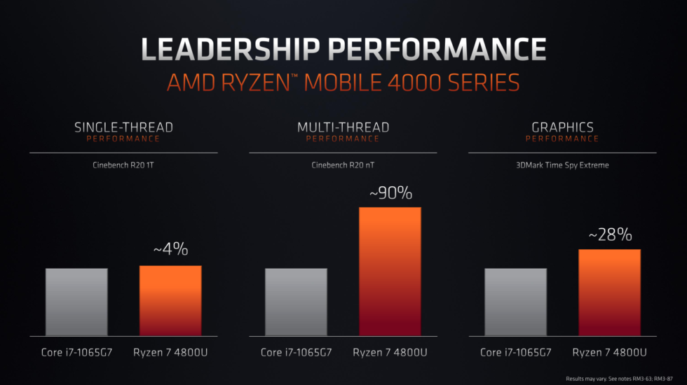
This ends up resulting in improved graphics performance with 8 CUs over the previously-used 11 CUs. This is quite a jump. I'm not quite sure what the 56% increase is in relation to but AMD's slides put graphics performance of the 4800U at 28% greater than the i7-1065G7 (Iris Plus 940) which is, in turn, around 23% greater than the UHD 620. The UHD 620 is approximately 58% faster than the 10 CUs in the 2700U which puts the 8 CUs in the 4800U at around 167% faster than the 2700U. That can be achieved due to the aforementioned improvements in efficiency as well as the shrink to the process node allowing much higher clock speeds.
Finally, the last sentence alludes to the fact that the three years working on these optimisations and these specific parts has also transferred over to Navi mobile parts.
In my opinion, this is a huge reveal.
 |
Being able to switch on and off parts of the die is supposedly very important for the next gen consoles' efficiency...
|
Up until now I've been speculating of a direct translation between desktop and console silicon for the graphics - purely due to the fact that we've had so little to go on. This simple-looking sentence from Dr. Su is deceptively full of information. These optimisations and benefits apparently do not affect curent Navi designs but will impact their mobile variations and (presumably) the Navi 2.0 silicon. In case you're not quite following along: consoles are essentially mobile chipsets...
One of the big things we've been seeing from the leaks of the next generation of consoles has been reportedly high GPU clock speeds, well in excess of what was achievable for the RX 5000 series. This has led outlets such as Digital Foundry to postulate that AMD/console manufacturers are really pushing the design envelopes for this silicon. The Ryzen 4000 series APUs seem to indicate that, actually, that may not be the case. In fact, 2 GHz GPU frequency might not be so outlandish or hard to reach!
The 4800U is hitting 1.75 GHz for 8 CUs at 15W TDP whereas the 2700U could do 1.3 GHz over 11 CUs at 45 W TDP. That's a BIG difference already... The 4800H can do 1.6 GHz at 45 W TDP but that's due to the 1.6x frequency of the CPU cores. If the TDP of a console was around 150-200 W then this limitation would fall away and 1.7 - 2.0 GHz could easily be in reach well below that... and that's using Vega!! The Navi architecture has a lot of optimisations that reduce the compute performance of the chipset but increase ROPs and other aspects of the graphics pipeline. This means that, as Digital Foundry found, Navi is more efficient per TFLOP than Vega (i.e. GCN).
It's incredibly interesting because we've also recently had a lot of physical evidence for the Xbox SX chip size which puts us at around 400 mm^2 according to WCCFTech and Digital Foundry.
 |
| WCCFTech's comparison between Scarlett and Scorpio... |
What's interesting here is that Anandtech have guesstimated the die size of the 8 core/8 CU Renoir chips at around 148 mm^2. That's actually pretty significant because it shows that 8 CUs, plus I/O, fit into an area of approximately 100 mm^2.
That's 74 mm^2 8 cores minus 24 MB L3 cache to give 47 mm^2 8 cores, 8 MB L3 cache. 148 mm^2 minus 47 mm^2 gives us the answer. Granted, we don't know how large the I/O is at 7 nm but a simple reduction of 2.60 from the 12LP nm process to a 7 nm process gives us an estimate of around 48 mm^2.
This could mean that 8 CUs fit into a die area of approximately 52 mm^2. Of course, it doesn't take into account the extra I/O required for integration between CPU and GPU but it's a general approximation.
If we do an incredibly simple (and by "simple" I mean, without much thought, as opposed to a complex mathematical calculation!) calculation, we see that approximately 46 CUs could exist in a 400 mm^2 die area once the reduced size 8 core CPU and I/O are taken into account.
46 CUs ia a potentially interesting number because at 2.0 GHz frequency, assuming parity in terms of performance with the desktop RX 5700 discrete graphics part, you achieve 12.50 TFLOPs. Now, Digital Foundry and other commentators and analysts are all about the redundancy in die design - and the industry precedent supports them on that premise... which could put us down to 42 CUs (4 CU buffer for duds) which puts us to 11.42 TFLOPs.
Now, that's pretty close to 12 TFLOPs and, given a little wiggle room due to optimisations, as we saw with mobile Vega 8 above, it's possible you could scrape by to 12 TFLOPs on 42 CUs.
Sure, the latest leak of the Xbox SX has it around 56 CUs but... is that really the final silicon or is it a dev kit? It's relatively common for developer kits to have more memory and/or CPU/GPU frequency than the final consumer release version of the consoles would have, so it's not without reason that leak might over-estimate the final design of the APU in Scarlett.
Switching over to the PS5, we just don't have enough information regarding that hardware to make any further inferences. Maybe in February with a Sony reveal or just before E3 but until then we're going to be in the dark once more... unless there are more leaks!
Ultimately, there's a long way to go through the rest of the year to the release windows of both consoles but it's really cool to see things firming up and seeing potential features from forked product stacks within AMD's arsenal applied to the next gen consoles themselves...
[UPDATE]
Whilst thinking about these things some more, I realised that the B8-coded chip designs for Renoir were 8-9 Compute Units - at least according to the leaks. This would improve yields for AMD on their binned parts since they have only announced chips with 8 CUs, giving them some leeway towards disabling one CU or accounting for an error in the silicon.
What this means is that, instead of 46 CUs crammed into an area corresponding to the remaining 304 mm^2 area of the SX SoC, you'd manage to fit in 52 CUs - 48 CUs with 4 redundant. 48 CUs would correspond to around 13.05 TFLOPs at a frequency of 2.0 GHz - putting us above the extrapolated 12 TFLOP performance numbers of the Xbox SX. Stepping the frequency back to something a bit more manageable, 1.8 GHz, you manage to achieve a 11.74 TFLOP number, very close to the magic "12 TFLOP".
Of course, since we're extrapolating numbers here there's no guarantee that the I/O is as small as I postulated above and the number of CUs could be fewer due to the increased functionality included in the RDNA2 architecture (Ray Tracing, for example). I also made a pretty big assumption that the 7 nm Vega CUs on Renoir were just a straight division from the area I calculated.
For comparison, Vega 20 (doing a straight division of 64 CUs per 331 mm^2 die area) gives us around 58 CUs - very similar to the reported 56 CU leak for the SX. However, those compute units are smaller and less optimised than Navi's are. Compare this with Navi 10 (40 CUs per 251 mm^2), we're back to around 48 CUs as I calculated for Renoir's improved Vega compute units.
Either way, I think from these numbers that 42-48 CUs could easily fit within the shown die area of the Xbox SX and, with a little optimisation and frequency adjustments, could easily hit 12 TFLOPs of compute performance. I would be suprised if the leaked 56 CU (+4 redundant) number was correct because it would require not only a significant reduction in CU size but wouldn't really line up with increased die area per CU to enable the improved features we expect from RDNA2.
I'm really interested to see how close to final specs we can get with these suppositions for the SX and I'm eagerly awaiting a lot more from the eventual PS5 reveal too. There was some speculation back in 2018 that AMD would be utilising SIMD in a different manner in their next generation architecture which at the time was sort of Navi/RDNA and sort of RDNA2. Moving forward, we had recent speculation based on a patent that was filed by SONY mentioning similar concepts.
The recent speculations appear to be under the impression that this changes the TFLOP calculation but I don't see how that can be the case and, as RedGamingTech pointed out in the response to this, the number of IPC is still 2, just potentially run at different frequencies on various CPU/GPU cores in the computing unit.
Added to this, SIMD is a feature of both GCN and RDNA - with RDNA specifically designed to reduce overhead by executing the operations on a shorter length of work-items, allowing for the improved performance of RDNA over GCN in graphics applications.
Barring any further leaks, the next entry in this series will include a look into how SONY might be implementing AMD's True Audio in the PS5...
46 CUs ia a potentially interesting number because at 2.0 GHz frequency, assuming parity in terms of performance with the desktop RX 5700 discrete graphics part, you achieve 12.50 TFLOPs. Now, Digital Foundry and other commentators and analysts are all about the redundancy in die design - and the industry precedent supports them on that premise... which could put us down to 42 CUs (4 CU buffer for duds) which puts us to 11.42 TFLOPs.
Now, that's pretty close to 12 TFLOPs and, given a little wiggle room due to optimisations, as we saw with mobile Vega 8 above, it's possible you could scrape by to 12 TFLOPs on 42 CUs.
Sure, the latest leak of the Xbox SX has it around 56 CUs but... is that really the final silicon or is it a dev kit? It's relatively common for developer kits to have more memory and/or CPU/GPU frequency than the final consumer release version of the consoles would have, so it's not without reason that leak might over-estimate the final design of the APU in Scarlett.
Switching over to the PS5, we just don't have enough information regarding that hardware to make any further inferences. Maybe in February with a Sony reveal or just before E3 but until then we're going to be in the dark once more... unless there are more leaks!
Ultimately, there's a long way to go through the rest of the year to the release windows of both consoles but it's really cool to see things firming up and seeing potential features from forked product stacks within AMD's arsenal applied to the next gen consoles themselves...
[UPDATE]
 |
| Vega 20 and Navi 10 both use TSMC's 7 nm process node. Can we use their CU sizes to do a better comparison? |
Whilst thinking about these things some more, I realised that the B8-coded chip designs for Renoir were 8-9 Compute Units - at least according to the leaks. This would improve yields for AMD on their binned parts since they have only announced chips with 8 CUs, giving them some leeway towards disabling one CU or accounting for an error in the silicon.
What this means is that, instead of 46 CUs crammed into an area corresponding to the remaining 304 mm^2 area of the SX SoC, you'd manage to fit in 52 CUs - 48 CUs with 4 redundant. 48 CUs would correspond to around 13.05 TFLOPs at a frequency of 2.0 GHz - putting us above the extrapolated 12 TFLOP performance numbers of the Xbox SX. Stepping the frequency back to something a bit more manageable, 1.8 GHz, you manage to achieve a 11.74 TFLOP number, very close to the magic "12 TFLOP".
Of course, since we're extrapolating numbers here there's no guarantee that the I/O is as small as I postulated above and the number of CUs could be fewer due to the increased functionality included in the RDNA2 architecture (Ray Tracing, for example). I also made a pretty big assumption that the 7 nm Vega CUs on Renoir were just a straight division from the area I calculated.
For comparison, Vega 20 (doing a straight division of 64 CUs per 331 mm^2 die area) gives us around 58 CUs - very similar to the reported 56 CU leak for the SX. However, those compute units are smaller and less optimised than Navi's are. Compare this with Navi 10 (40 CUs per 251 mm^2), we're back to around 48 CUs as I calculated for Renoir's improved Vega compute units.
Either way, I think from these numbers that 42-48 CUs could easily fit within the shown die area of the Xbox SX and, with a little optimisation and frequency adjustments, could easily hit 12 TFLOPs of compute performance. I would be suprised if the leaked 56 CU (+4 redundant) number was correct because it would require not only a significant reduction in CU size but wouldn't really line up with increased die area per CU to enable the improved features we expect from RDNA2.
I'm really interested to see how close to final specs we can get with these suppositions for the SX and I'm eagerly awaiting a lot more from the eventual PS5 reveal too. There was some speculation back in 2018 that AMD would be utilising SIMD in a different manner in their next generation architecture which at the time was sort of Navi/RDNA and sort of RDNA2. Moving forward, we had recent speculation based on a patent that was filed by SONY mentioning similar concepts.
The recent speculations appear to be under the impression that this changes the TFLOP calculation but I don't see how that can be the case and, as RedGamingTech pointed out in the response to this, the number of IPC is still 2, just potentially run at different frequencies on various CPU/GPU cores in the computing unit.
 |
An excerpt from the RDNA whitepaper linked above showing how RDNA is almost 2 times faster than GCN at executing an instruction by reducing the work-item by half but doubling the number of computations in a single Compute Unit (CU). |
Barring any further leaks, the next entry in this series will include a look into how SONY might be implementing AMD's True Audio in the PS5...
No comments:
Post a Comment